減速法
減速法
deceleration method
[目次:装置]
低加速電圧でのSEM像の空間分解能を高く保つために、試料への照射直前で電子線を、電場を用いて減速させる方法。特に~1 keV以下の低加速電子線を試料に照射して観察する際に、高い空間分解能を保持する効果が大きい。低加速電子線は試料の最表面を観察する場合や、高分子材料のように高加速電子線でダメージを受けやすい試料や帯電しやすい試料を観察する場合に用いられる。
入射電子線を減速させるための電場 (以下、単に減速電場と呼ぶ) の発生方法には、リターディング法とブースティング法がある (図1)。ブースティング法では鏡筒内に加速管を設置する必要がある。リターディング法は試料に電位を与えることができれば減速できるため、加速管の設置は必要ない。数100 Vの極低加速条件で高い空間分解能でSEM観察を行う場合には、ブースティング法にリターディング法を追加した手法が用いられる。図1は電子線を3 keVから1 keVに減速した例である。ここでは、図1の例に基づいてリターディング法とブースティング法のそれぞれについて説明する。
リターディング法 (図1 (a))では試料に負電位 (-2 kV) を印加する。3 keVで放出された電子線は対物レンズ内を3 keVのまま通過し、レンズと試料の間で1 keVまでに減速される。ブースティング法 (図1 (b)) では、鏡筒内に設けた加速管に正の電位 (+2 kV) を印加する。1 keVで放出された電子線は加速管で3 keVまで加速される。電子線は対物レンズ内を3 keVで通過し、加速管の出口と対物レンズの下端の間で1 keVまで減速され、試料に照射される。
減速法を用いると、1) 入射電子線を高い電圧で対物磁場レンズを通せるため、対物レンズによる色収差を小さくすることができ、電子プローブの径が小さくなる。2) 発生させた減速電場が付加的な凸レンズとして働き、レンズ全体の中心 (主面) の位置が試料に近づく。その結果、さらに電子プローブの径が小さくなる。3) 付加的な電場レンズによる色収差は電子プローブの径を大きくする。1)、2) の寄与によってSEM像の空間分解能が向上する。特に1) の効果が分解能の向上に大きく寄与している。
図2に (a) 減速電場なし、(b) リターディング法および (c) ブースティング法の電子線の軌道をそれぞれ模式的に示した。減速法を用いると、電子線は磁場レンズ中を3 keV (1 keVではなく) で通過して、その後、減速電場で1 keVに減速されて試料に集束する。磁場レンズ中を通る電子線のエネルギーが高いことによって、磁場レンズによる色収差を小さく抑えることができる。さらに、電子線は減速電場内を進むにつれて減速し、軌道の傾きを増しながら試料面上に集束する。入射電子の軌道を延長した破線Aと試料面での軌道の接線 (破線B) との交点は主面位置を与える。減速電場により、レンズの主面の位置が下がり焦点距離が短くなり、レンズの縮小率が上がる。
表1は、図1および2で示した各モデルで実現される電子プローブ径dとそれを構成する成分do,, dc,, dd, dsの大きさについて計算した結果である。減速電場を用いずに低加速 (1 keV) の電子線で結像した場合は、収差成分の内、色収差の径成分dcおよび回折収差の径成分ddでプローブ径の大きさがほぼ決まる[1]。減速法を用いると対物レンズの色収差が減ることによってdcが減る。さらに、縮小率 (集束角) が上がるために光源成分doと回折収差による成分ddが小さくなる。
リターディング法では試料に凹凸がある場合や試料に傾きがある場合には、試料の直前の電場が乱れるため分解能の劣化やコントラストの異常を引き起こすという短所がある。一方で、ブースティング法とリターディング法を組み合わせることで、数100 Vの極低加速電圧でも高い空間分解能 (プローブ径を最小の状態にして) でSEM観察ができる。
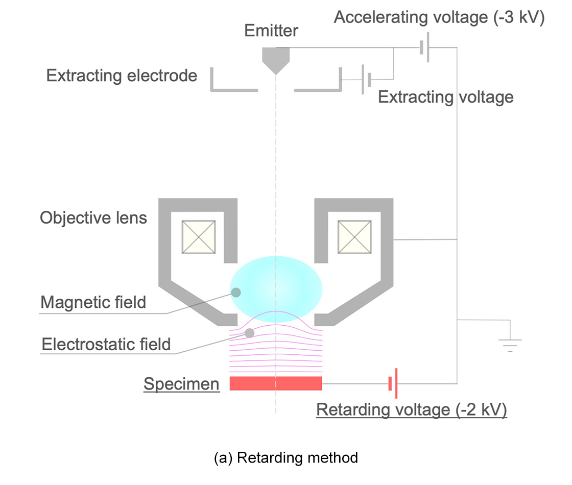
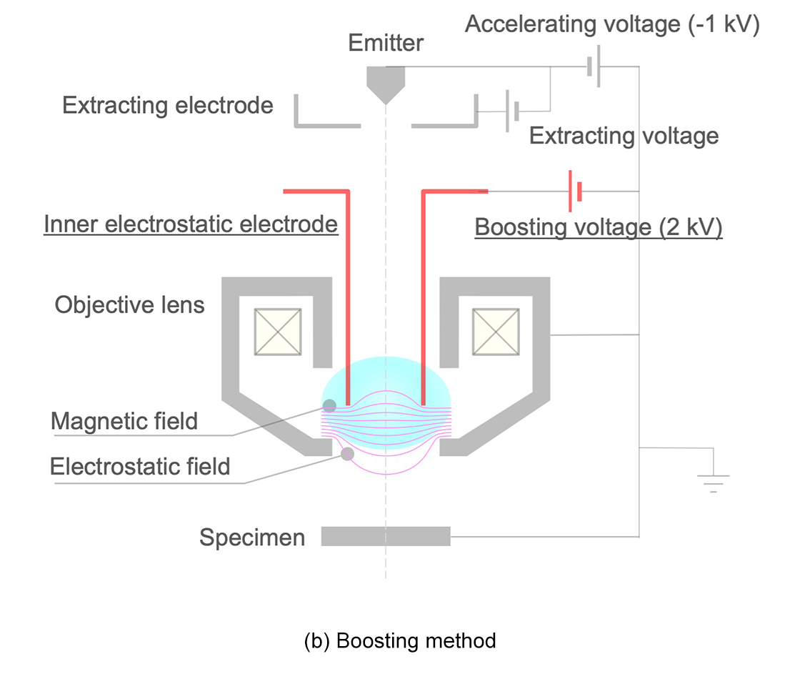
図1 減速法の種類と構成図
電子線を3 keVから1 keVに減速した場合について示している。
(a) リターディング法。試料に対物レンズに対して負の電圧 (この例では-2 kV) を印加し対物レンズの下極と試料との間に減速電場を発生させる。
(b) ブースティング法。鏡筒内の電子線通路に設けた加速管に正の電圧 (この例では2 kV) を印加し、加速管の下端と対物レンズの下極との間に減速電場を発生させる。ブースティング法には、加速管を備えた専用の装置が必要になる。加速管を備えた装置に、試料に電位を印加できるようにすれば、ブースティング法とリターディング法を併用することができる。
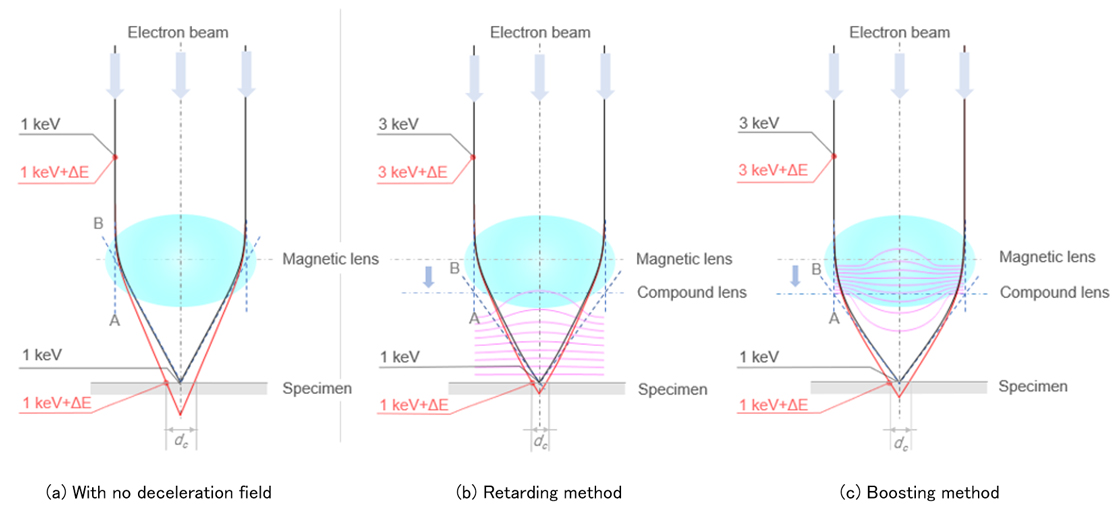
図2 減速法での電子線軌道図 (入射電子線エネルギー1 keV)
試料入射電子線エネルギー1 [keV] および1 + ΔE [keV] の電子軌道をそれぞれ黒線、赤線で示した。
(a) 減速法を用いない場合。(b) リターディング法および (c) ブースティング法。(a) 減速法を用いない場合の主面は図中 "Magnetic lens" とラベルした鎖線上に位置する。黒線と赤線のズレの大きさは色収差による焦点位置のズレによる。試料位置での水平方向の幅は色収差によるプローブ径成分に相当する。複合レンズの主面位置は "Compound lens" とラベルした鎖線上に位置し、(a) 減速法を用いない場合の主面から下に移動していることがわかる。黒線と赤線のズレの小ささは色収差が低減したことを示す。試料面上で1 keVの電子軌道 (黒線) に引いた接線の傾きから開き角が求まる。減速法を用いた場合、減速電場の影響により開き角が増加している。
表1 電子プローブ径の計算値†
| 各プローブ径成分 [nm] | 減速電場なし | リターディング法 | ブースティング法 |
|---|---|---|---|
光源成分![do = Mdss [nm]](./glossary_file/file/deceleration-optics_4.png) |
8.3 | 6.0 | 5.9 |
回折収差成分![dd = 0.61λ⁄sinα [nm]](./glossary_file/file/deceleration-optics_5.png) |
6.9 | 5.0 | 4.9 |
球面収差成分![ds = 0.5Csα3 [nm]](./glossary_file/file/deceleration-optics_6.png) |
0.68 | 0.79 | 0.76 |
色収差成分![dc =Cc ∆E⁄Eα [nm]](./glossary_file/file/deceleration-optics_7.png) |
11 | 4.8 | 6.9 |
電子プローブ径![d = √(d02+dd2+ds2+dc2) [nm]](./glossary_file/file/deceleration-optics_8.png) |
15 | 9.3 | 10 |
† ここでMは縮小率、dssは光源の大きさ、λは電子線の波長、αは開き角、ΔEは電子線のエネルギー幅、Eは電子線の運動エネルギーをそれぞれ表す。
[1] SEMの用語集 "電子プローブ径" を参照のこと。図2に低速条件では色収差、回折収差が支配的であることが示されている。
A method of decelerating the incident electron beam just before a specimen using an electric field, so as to maintain a high spatial resolution of the SEM image at a low accelerating voltage. The method is particularly effective in maintaining high spatial resolution for the low-accelerated electron beam of ~1 keV or less. The low-accelerated electron beam is used to observe the top surface of a specimen, and to observe specimens which are easily damaged by a high-accelerated electron beam, such as polymer materials, and specimens which are easily electrically charged.
There are two methods of generating an electrostatic field to decelerate the incident electron beam (hereinafter, called "deceleration field"): the retarding method and boosting method (Fig. 1). In the boosting method, the accelerating tube has to be placed in the microscope column. In the retarding method, the incident beam can be decelerated by applying a potential directly to the specimen without installing the accelerating tube. For a high spatial-resolution SEM observation at an extremely low accelerating voltage of a few 100 V, the retarding method is used in addition to the boosting method. The two methods are explained for the examples shown in Fig. 1, where the electron beam is decelerated from 3 keV down to 1 keV.
In the retarding method (Fig. 1 (a)), a negative voltage of -2 kV is applied to the specimen. An electron beam emitted at 3 keV passes through the objective lens at 3 keV, and then the electron beam is decelerated down to 1 keV between the objective lens and specimen.
In the boosting method (Fig. 1 (b)), a positive voltage of +2 kV is applied to the accelerating tube placed in the microscope column. An electron beam emitted at 1 keV is accelerated up to 3 keV in the accelerating tube and passes through the objective lens at 3 keV. Then, the electron beam is decelerated down to 1 keV between the exit of the accelerating tube and the lower pole of the objective lens, and then reaches the specimen.
When using the deceleration method, 1) The incident electron beam passes though the magnetic field of the objective lens at a high voltage and thus, the chromatic aberration of the objective lens is reduced, leading to a decrease of the electron-probe diameter. 2) The deceleration field acts as an additional convex lens and thus, the center (principal plane) of the entire lens comes closer to the specimen, leading the probe diameter even smaller. 3) The chromatic aberration of the electrostatic lens increases the probe diameter.
The effects of 1) and 2) contribute to improve the spatial resolution of the SEM image. In particular, the effect of 1) contributes significantly to the improvement of the spatial resolution.
Fig. 2 schematically shows the trajectories of the electron beam for (a) no deceleration filed, (b) the retarding method, and (c) the boosting method. When the deceleration method is used, the electron beam passes through the magnetic objective lens at 3 keV (not 1 keV) and is then decelerated to 1 keV by the electrostatic field, and converges onto the specimen. To maintain the energy of the electron beam high in the magnetic lens allows the chromatic aberration of the magnetic lens to be small. Furthermore, as the electron beam travels through the deceleration field, the beam is decelerated and converges onto the specimen plane with increasing the inclination of the electron trajectory. In each figure (a and b), the intersection point of the dashed line A extending the incident beam with the tangential line (dashed line B) of the trajectory on the specimen plane, gives the position of the principal plane. The deceleration field lowers the principal-plane of the lens and shorten the focal length, increasing the demagnification ratio of the lens.
Table 1 lists the calculated electron-probe diameters d and the magnitudes of their components do,, dc,, dd, ds achieved for the three models shown in Fig. 1 and Fig. 2. In the case of imaging with a low acceleration energy of 1 keV with no deceleration field, the probe diameter is almost determined by the diameter components of chromatic aberration dc and diffraction aberration dd [1]. When the deceleration method is used, dc decreases owing to the decrease of chromatic aberration of the objective lens. Furthermore, since the demagnification ratio (convergence angle) is increased, the electron source component d0 and diffraction aberration component of dd. decrease.
In the retarding method, if the specimen is uneven or tilted, the electric field in front of the specimen can be disturbed and then, a degradation of resolution may occur and anomalous contrast may arise.
Combining the bosting method and the retarding method, the highest spatial-resolution SEM image (the smallest probe diameter) can be obtained at extremely low accelerating voltages of a few 100 V.
Fig. 1 Two deceleration methods (schematics)
The case of an electron beam being decelerated from 3 keV down to 1 keV is shown.
(a) Retarding method. A negative voltage (-2 kV) is applied to the specimen with respect to the objective lens, and a deceleration field is generated between the lower pole of the objective lens and the specimen.
(b) Boosting method. A positive voltage (2 kV) is applied to the accelerating tube in the electron-beam path, and a deceleration field is generated between the lower end of the tube and the lower pole of the objective lens. The boosting method requires a dedicated instrument with an accelerating tube.
A combined use of the boosting and retarding methods is possible if the instrument with the accelerating tube is designed to make it possible to apply a potential to the specimen.
Fig. 2 Electron-beam trajectories in the deceleration methods (landing electron-beam energy: 1 keV)
The electron-beam trajectories for the landing electron-beam energy of 1 keV and of 1 + ΔE keV are respectively shown by black lines and red lines. (a) Without the deceleration method. (b) With the retarding method and (c) with the boosting method. (a) When the deceleration method is not used, the principal plane of the lens is located on the dashed line labelled as "Magnetic lens" in the figure. The shift between the black line and red line is due to the shift of the focal point caused by the chromatic aberration of the lens. The size (width) of the red line on the specimen corresponds to the probe-diameter component due to the chromatic aberration. The position of the principal plane of the compound lens composed of the magnetic field and the electrostatic field, each shown in (b) and (c), is on the dashed line labelled as "Compound lens" in each figure. The position of the principal plane using the deceleration method, is shifted downward from the position without the deceleration method (a). The deviation between the black line and red line shown in (b) and (c) is smaller than that from (a). This indicates that the chromatic aberration is reduced when the deceleration method is used. The convergence angle of the electron beam onto the specimen is determined by the tangential line of the electron trajectory (black line) at 1 keV on the specimen plane. When the deceleration method is used, the convergence angle increases owing to the lens action by the deceleration field.
Table 1 Calculations of the electron-probe diameters without the deceleration method and with two deceleration methods †
| Probe diameter component [nm] | Without deceleration field | Retarding method | Boosting method |
|---|---|---|---|
| Electron source component |
8.3 | 6.0 | 5.9 |
| Diffraction aberration component |
6.9 | 5.0 | 4.9 |
| Spherical aberration component |
0.68 | 0.79 | 0.76 |
| Chromatic aberration component |
11 | 4.8 | 6.9 |
| Electron-probe diameter |
15 | 9.3 | 10 |
† Here, M is the demagnification ratio, dss is the electron source size, λ is the wavelength of the electron, α is the convergence angle, ΔE is the energy spread of the electron, and E is the energy of the electron.
[1] It is noted that the chromatic aberration and diffraction aberration are dominant at a low accelerating voltage condition (see Fig. 2 of "electron-probe diameter" in "Glossary of SEM Terms." of JEOL Web site).
関連用語から探す
説明に「減速法」が含まれている用語


